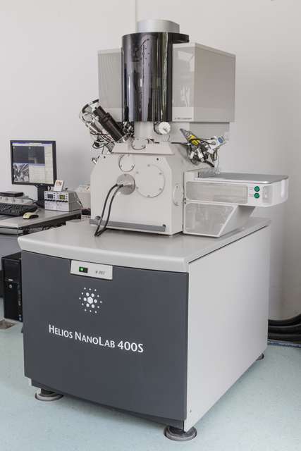
FEI Helios NanoLab 400S FIB-SEM (FIB 400)
Jülich
The FEI Helios NanoLab 400S FIB-SEM is one of the world’s most advanced DualBeamTM focused ion beam (FIB) platforms for transmission electron microscopy (TEM) sample preparation, scanning electron microscopy (SEM) imaging and analysis in semiconductor failure analysis, process development and process control. The FEI Helios NanoLab 400S FIB-SEM combines an ElstarTM electron column for high-resolution and high-contrast imaging with a high-performance SidewinderM ion column for fast and precise cross sectioning. The FEI Helios NanoLab M 400S is optimised for high throughput high-resolution S/TEM sample preparation, SEM imaging and energy dispersive X-ray analysis. Its exclusive FlipStageTM and in situ STEM detector can flip from sample preparation to STEM imaging in seconds without breaking vacuum or exposing the sample to the environment. Platinum gas chemistry is the preferred metal deposition when a high deposition rate and precision of the deposition are required. Carbon deposition can be chosen as well. The system additionally allows for spatially resolved compositional analysis using the attached EDAX Genesis XM 4i X-ray microanalysis system.
Typical Applications and Limitations of Use
The configuration of the FEI Helios NanoLab 400S allows a variety of advanced imaging and preparation techniques to be applied to wide bunch of solid state materials. These techniques include TEM sample preparation (normal- and backside milling) without breaking the vacuum, STEM imaging on thin TEM samples, slice and view operation (automatic), needle preparation for tomography, plan-view preparation and the preparation of lamellas on heating chips for TEM annealing experiments.
The FEI Helios NanoLab 400S is not intended for the investigation of aqueous, ferromagnetic or organic samples without further discussions with both of the instruments officers and the ER-C general management.
Link: https://er-c.org/index.php/access/
